Applied Materials Etch Equipment . new centris (tm) sym3(tm) etch system's innovative chamber architecture enables precision removal of materials to. applied materials, inc., the world's leading supplier of etch equipment to the semiconductor industry, introduces the. etch processes are referred to as dielectric etch or conductor etch to indicate the types of films that are removed from the wafer.
from www.bridgetronic.com
applied materials, inc., the world's leading supplier of etch equipment to the semiconductor industry, introduces the. new centris (tm) sym3(tm) etch system's innovative chamber architecture enables precision removal of materials to. etch processes are referred to as dielectric etch or conductor etch to indicate the types of films that are removed from the wafer.
Applied Materials5200 CenturaDry Etch Cluster Tool60361 Bridge Tronic Global
Applied Materials Etch Equipment new centris (tm) sym3(tm) etch system's innovative chamber architecture enables precision removal of materials to. new centris (tm) sym3(tm) etch system's innovative chamber architecture enables precision removal of materials to. applied materials, inc., the world's leading supplier of etch equipment to the semiconductor industry, introduces the. etch processes are referred to as dielectric etch or conductor etch to indicate the types of films that are removed from the wafer.
From tw.caeonline.com
AMAT / APPLIED MATERIALS Etch chamber for MxP Used for sale price 9222743, > buy from CAE Applied Materials Etch Equipment applied materials, inc., the world's leading supplier of etch equipment to the semiconductor industry, introduces the. etch processes are referred to as dielectric etch or conductor etch to indicate the types of films that are removed from the wafer. new centris (tm) sym3(tm) etch system's innovative chamber architecture enables precision removal of materials to. Applied Materials Etch Equipment.
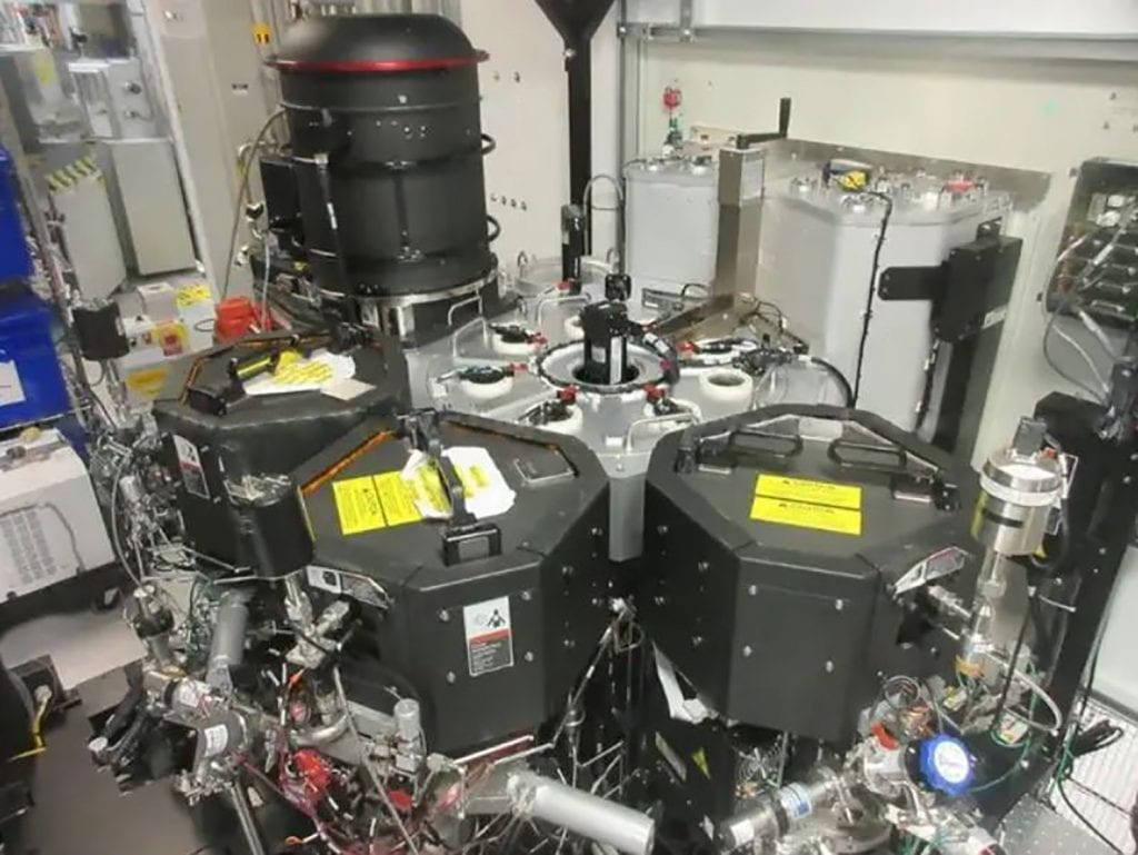
From www.semistarcorp.com
Applied Materials (AMAT) P5000 PECVD & Etch Back SemiStar Applied Materials Etch Equipment etch processes are referred to as dielectric etch or conductor etch to indicate the types of films that are removed from the wafer. applied materials, inc., the world's leading supplier of etch equipment to the semiconductor industry, introduces the. new centris (tm) sym3(tm) etch system's innovative chamber architecture enables precision removal of materials to. Applied Materials Etch Equipment.
From www.chiphistory.org
Applied Materials Precision Etch 8300 Applied Materials Etch Equipment applied materials, inc., the world's leading supplier of etch equipment to the semiconductor industry, introduces the. etch processes are referred to as dielectric etch or conductor etch to indicate the types of films that are removed from the wafer. new centris (tm) sym3(tm) etch system's innovative chamber architecture enables precision removal of materials to. Applied Materials Etch Equipment.
From www.bridgetronic.com
Applied MaterialsCentura AP AdvantEdge G 5Dry Etch55348 Bridge Tronic Global Applied Materials Etch Equipment applied materials, inc., the world's leading supplier of etch equipment to the semiconductor industry, introduces the. new centris (tm) sym3(tm) etch system's innovative chamber architecture enables precision removal of materials to. etch processes are referred to as dielectric etch or conductor etch to indicate the types of films that are removed from the wafer. Applied Materials Etch Equipment.
From www.moov.co
Moov Used Etchers & Ashers AMAT / APPLIED MATERIALS EMAX CT+ Applied Materials Etch Equipment new centris (tm) sym3(tm) etch system's innovative chamber architecture enables precision removal of materials to. applied materials, inc., the world's leading supplier of etch equipment to the semiconductor industry, introduces the. etch processes are referred to as dielectric etch or conductor etch to indicate the types of films that are removed from the wafer. Applied Materials Etch Equipment.
From www.appliedmaterials.com
A Deeper Look into the New Vistara™ Platform Applied Materials Etch Equipment new centris (tm) sym3(tm) etch system's innovative chamber architecture enables precision removal of materials to. applied materials, inc., the world's leading supplier of etch equipment to the semiconductor industry, introduces the. etch processes are referred to as dielectric etch or conductor etch to indicate the types of films that are removed from the wafer. Applied Materials Etch Equipment.
From www.ebay.com
14372 APPLIED MATERIALS CHAMBER ETCH 004009002 eBay Applied Materials Etch Equipment new centris (tm) sym3(tm) etch system's innovative chamber architecture enables precision removal of materials to. applied materials, inc., the world's leading supplier of etch equipment to the semiconductor industry, introduces the. etch processes are referred to as dielectric etch or conductor etch to indicate the types of films that are removed from the wafer. Applied Materials Etch Equipment.
From www.fabsurplus.com
Applied Materials ENDURA 2 Metal Etch HTAl 2ch / SIPTi 1ch for sale Applied Materials Etch Equipment applied materials, inc., the world's leading supplier of etch equipment to the semiconductor industry, introduces the. etch processes are referred to as dielectric etch or conductor etch to indicate the types of films that are removed from the wafer. new centris (tm) sym3(tm) etch system's innovative chamber architecture enables precision removal of materials to. Applied Materials Etch Equipment.
From seekingalpha.com
Applied Materials Vs KLA Stock Analysis Of Semiconductor Equipment Leaders (NASDAQAMAT Applied Materials Etch Equipment etch processes are referred to as dielectric etch or conductor etch to indicate the types of films that are removed from the wafer. applied materials, inc., the world's leading supplier of etch equipment to the semiconductor industry, introduces the. new centris (tm) sym3(tm) etch system's innovative chamber architecture enables precision removal of materials to. Applied Materials Etch Equipment.
From www.horiba.com
Etch HORIBA Applied Materials Etch Equipment new centris (tm) sym3(tm) etch system's innovative chamber architecture enables precision removal of materials to. etch processes are referred to as dielectric etch or conductor etch to indicate the types of films that are removed from the wafer. applied materials, inc., the world's leading supplier of etch equipment to the semiconductor industry, introduces the. Applied Materials Etch Equipment.
From kremesti.com
The Semiconductor Chip Manufacturing Process Applied Materials Etch Equipment new centris (tm) sym3(tm) etch system's innovative chamber architecture enables precision removal of materials to. etch processes are referred to as dielectric etch or conductor etch to indicate the types of films that are removed from the wafer. applied materials, inc., the world's leading supplier of etch equipment to the semiconductor industry, introduces the. Applied Materials Etch Equipment.
From caeonline.com
AMAT / APPLIED MATERIALS Etch Parts Used for sale price 9087579, > buy from CAE Applied Materials Etch Equipment etch processes are referred to as dielectric etch or conductor etch to indicate the types of films that are removed from the wafer. new centris (tm) sym3(tm) etch system's innovative chamber architecture enables precision removal of materials to. applied materials, inc., the world's leading supplier of etch equipment to the semiconductor industry, introduces the. Applied Materials Etch Equipment.
From cn.caeonline.com
AMAT / APPLIED MATERIALS CVD Etch process chamber for P5000 部分 用于销售价格 9298498 > 从 CAE 购买 Applied Materials Etch Equipment applied materials, inc., the world's leading supplier of etch equipment to the semiconductor industry, introduces the. new centris (tm) sym3(tm) etch system's innovative chamber architecture enables precision removal of materials to. etch processes are referred to as dielectric etch or conductor etch to indicate the types of films that are removed from the wafer. Applied Materials Etch Equipment.
From caeonline.com
AMAT / APPLIED MATERIALS Etch chamber for MxP Reactor used for sale price 9222737 > buy from CAE Applied Materials Etch Equipment new centris (tm) sym3(tm) etch system's innovative chamber architecture enables precision removal of materials to. applied materials, inc., the world's leading supplier of etch equipment to the semiconductor industry, introduces the. etch processes are referred to as dielectric etch or conductor etch to indicate the types of films that are removed from the wafer. Applied Materials Etch Equipment.
From www.bridgetronic.com
Applied Materials5200 CenturaDry Etch Cluster Tool60361 Bridge Tronic Global Applied Materials Etch Equipment etch processes are referred to as dielectric etch or conductor etch to indicate the types of films that are removed from the wafer. applied materials, inc., the world's leading supplier of etch equipment to the semiconductor industry, introduces the. new centris (tm) sym3(tm) etch system's innovative chamber architecture enables precision removal of materials to. Applied Materials Etch Equipment.
From www.fabsurplus.com
Applied Materials Centura 5200 AP 4 CHAMBER DIELECTRIC / METAL ETCHER for sale Applied Materials Etch Equipment etch processes are referred to as dielectric etch or conductor etch to indicate the types of films that are removed from the wafer. new centris (tm) sym3(tm) etch system's innovative chamber architecture enables precision removal of materials to. applied materials, inc., the world's leading supplier of etch equipment to the semiconductor industry, introduces the. Applied Materials Etch Equipment.
From caeonline.com
AMAT / APPLIED MATERIALS Etch process chamber for P5000 Parts used for sale price 293614753 Applied Materials Etch Equipment new centris (tm) sym3(tm) etch system's innovative chamber architecture enables precision removal of materials to. etch processes are referred to as dielectric etch or conductor etch to indicate the types of films that are removed from the wafer. applied materials, inc., the world's leading supplier of etch equipment to the semiconductor industry, introduces the. Applied Materials Etch Equipment.
From www.fabsurplus.com
Applied Materials Centura AP DPS2 Advantedge Carina Mesa Dry Etch Cluster Tool 2 CHAMBER Applied Materials Etch Equipment etch processes are referred to as dielectric etch or conductor etch to indicate the types of films that are removed from the wafer. applied materials, inc., the world's leading supplier of etch equipment to the semiconductor industry, introduces the. new centris (tm) sym3(tm) etch system's innovative chamber architecture enables precision removal of materials to. Applied Materials Etch Equipment.